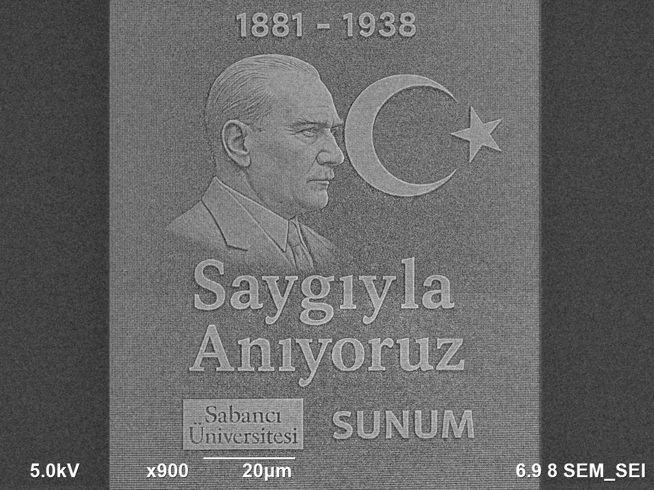
For the commemoration of November 10, SUNUM Technical Team created a special design that was first prepared in 8-bit grayscale format. The image was then processed using BEAMER (GenISys) software and divided into 256 layers, generating a GPF file ready for electron beam writing. A PMMA 950 A9 e-beam resist was spin-coated onto a silicon substrate, and the pattern was written using the Raith EBPG5000plusES 100 kV Electron Beam Lithography System. By applying different exposure doses for each layer, the image was fabricated on the substrate as a three-dimensional microscale structure. After exposure, the resist was developed using a PMMA developer. To prevent charging during SEM imaging, the surface was coated with a 20 nm Pd/Au thin film via sputtering. Finally, the sample was imaged using the JEOL JIB-4601 MultiBeam FIB-SEM system under 5 kV.
This work was carried out using the SUNUM infrastructure, demonstrating the combination of science and technology in a 3D microscale design dedicated to the memory of November 10.

