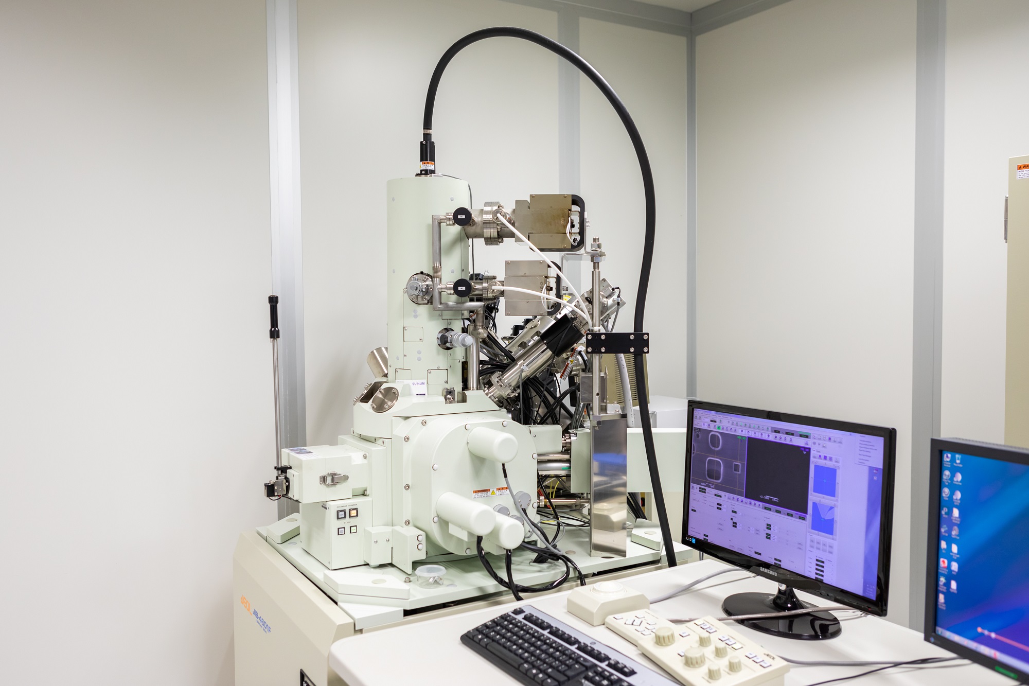
In the Measurement and Imaging Laboratory at SUNUM Sabancı University Nanotechnology Research and Application Center, the High-Resolution Transmission Electron Microscope (HR-TEM) enables imaging at atomic resolution, crystal structure determination, and chemical analysis. With its superior resolution and advanced analytical capabilities, it offers a wide range of applications in advanced materials research, nanotechnology, semiconductors, and more. The microscope is equipped with Energy Dispersive X-ray Spectroscopy (EDS) and Electron Energy Loss Spectroscopy (EELS), allowing for the identification of material elements, creation of distribution maps, and analysis of chemical composition.
The SEM system in our Electron Microscopy Laboratory is equipped with SE (Secondary Electron) and EDS/BSE (Energy Dispersive X-ray Spectroscopy/Back Scattered Electron) detectors (Oxford Xmax-N EDS System). The SEM allows for imaging of materials' micro/nano-scale surface morphology and microstructure using SE and BSE detectors; while the EDS system is used for qualitative and quantitative chemical analysis. High-resolution imaging, information on surface morphology and topography, shape and size analysis, EDS spectral analysis, and EDS mapping are performed with high precision and advanced expertise across a wide range of materials, from polymers to metals, both hard and soft.
The Cryo-Ultramicrotome System allows for the high-precision sectioning of both biological and industrial materials without deformation, using PowerTome Ultramicrotome devices and the LN Ultra-Cryo attachment cooled with liquid nitrogen. The system's two different stages allow for sectioning at both room temperature and cryo conditions. Optimal thermal stability for cryosectioning is achieved with the LN Ultra-Cryo attachment mounted on the PowerTome. The stable sample chamber of the LN Ultra enables work with a wide variety of sample types, ranging from +40°C to -185°C, including rubbers, soft polymers, and biological cells and tissues. The system enables the preparation of ultrathin sections (<100>
Before electron microscopy work, the surfaces of insulating samples are made conductive by coating them with thin conductive films using the sputter technique. For this purpose, our laboratory is equipped with Metal (Au/Pd) and Carbon Sputter Coaters.
For information and reservations : sunum-services@sabanciuniv.edu
For devices and services: sunum.sabanciuniv.edu

